Classification and principle of image sensors
The imaging objective lens images (or self luminous) objects illuminated by external lighting on the image plane of the objective lens to form a two-dimensional spatial light intensity distribution (optical image). The sensor that can convert the optical image of the two-dimensional light intensity distribution into a one-dimensional sequential electrical signal is called an image sensor.

According to different components, image sensors can generally be divided into:
- CCD (Charge Coupled Device)
- CMOS (Complex Metal Oxide Semiconductor)
- CIS (contact image sensor)
1、charge coupled device
As a solid-state image sensor, CCD has a series of advantages, such as small volume, light weight, high resolution, high sensitivity, wide dynamic range, high geometric accuracy of photosensitive element, wide spectral response range, low operating voltage, low power consumption, long life, good shock resistance and shock resistance, free from electromagnetic interference and high reliability.
There are many indicators to evaluate a CCD sensor, such as the number of pixels, CCD size, signal to noise ratio, and so on. Among them, the number of pixels and the size of CCD are the most important indicators, and the number of pixels refers to the number of sensitive elements on the CCD.
We can understand the captured picture as many small points, each point is a pixel. Obviously, the more pixels, the clearer the picture will be. If the CCD does not have enough pixels, the sharpness of the captured picture will be greatly affected.
Therefore, the more pixels of CCD, the better. However, in order to obtain better picture quality, the increase of the number of pixels of CCD will inevitably lead to a problem, that is, the increase of CCD manufacturing cost and the decline of yield.

2. CMOS metal oxide semiconductor device
CMOS image sensor is a typical solid imaging sensor, which has the same historical origin with CCD. CMOS image sensor is usually composed of image sensor array, row driver, column driver, timing control logic, AD converter, data bus output interface, control interface, na kadhalika.
These parts are usually integrated on the same silicon chip, and its working process can generally be divided into reset, photoelectric conversion, integration, and readout parts.
The photoelectric information conversion function of CMOS is basically similar to that of CCD, but the difference lies in the different ways of information transmission after photoelectric conversion of these two sensors.
CMOS has the characteristics of simple way to read information, fast output information rate, low power consumption (only about 1/10 of the CCD chip), small size, light weight, high integration and low price.
In terms of manufacturing process, CCD manufacturing process is relatively complex. Only a few manufacturers, such as Sony, Panasonic and Sharp, master this technology, so the price of CCD cameras will be relatively expensive.
In fact, after technical transformation, the gap between the actual effect of CCD and advanced CMOS has been very small, and the manufacturing cost and power consumption of CMOS are lower than CCD, so many camera manufacturers use CMOS light-sensitive components as the core components.
Several well-known manufacturers have also increased the research and development of CMOS sensors since 2000. At present, the growth rate of CMOS has reached several times the level of CCD. In the digital cameras launched by Nikon, Sony or Canon in recent years, we can hardly see the trace of CCD.
In the future, the main development direction of the camera market will still be to take CMOS as the core, and constantly improve the resolution and sensitivity of CMOS on this basis.
3. CIS contact image sensor
CIS is generally used in scanners. As it is contact scanning (it must be kept very close to the original), only LED light source can be used, and its depth of field, resolution and color performance can not catch up with the CCD sensor at present, nor can it be used to scan the transmission film.
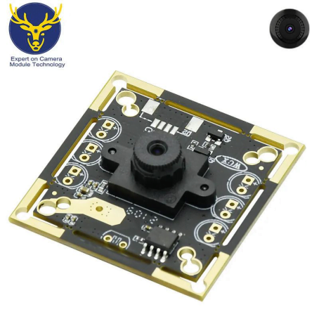
Shenzhen Jinshikang Technology focuses on the R&D, production and sales of camera modules. The module products produced adopt CMOS image sensor technology. The information reading mode is simple, the output information rate is fast, the power consumption is low, the volume is small, the weight is light, the integration is high, and the cost is low. Welcome to consult, investigate and cooperate.
Classification and principle of image sensors Classification and principle of image sensors Classification and principle of image sensors Classification and principle of image sensors Classification and principle of image sensors Classification and principle of image sensors Classification and principle of image sensors Classification and principle of image sensors
